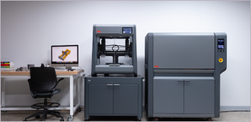
Nano Dimension makes DragonFly, a multimaterial, multilayer 3D printer that can generate entire circuits in one step, including substrate, conductive traces and passive components. Image courtesy of Nano Dimension.


Latest News
September 28, 2022
Using 3D printing to create an operational electronic device in one pass may sound like science fiction, but it is quickly becoming a reality. Academic researchers and additive manufacturing (AM) startups call it 3D electronics, and they are making considerable progress in bringing it to market.
IDTechEx, a market research firm with AM in its portfolio, broadly defines 3D electronics as any additive method that enables separately manufactured printed circuit boards (PCBs) to be replaced with integrated electronics. To be viable for industry, such methods must save space and weight, and reduce manufacturing complexity.
“With 3D Electronics, adding electronic functionality no longer requires incorporating a rigid, planar PCB into an object then wiring up the relevant switches, sensors, power sources and other external components,” the company says in an overview of the field.
Matthew Dyson, a senior analyst at IDTechEx, says the concept of 3D electronics is divided into three parts. The first involves applying electronics onto the surface of a 3D printed part. Second is the printing of fully additive, fully printed electronics built up layer by layer. Third is to make an electronic component and then do AM around it, possibly in conjunction with other manufacturing methods such as molding. This method is sometimes called in-mold electronics.
It is already possible to add antennas and other simple conductive interconnects to the surface of injected molded plastic objects. Complexity is increasing thanks to innovations in materials and processes.
Applying Electronics to a Surface
Laser direct structuring (LDS), around for more than a decade, is currently the primary method for using AM to add electronics to an object. IDTechEx estimates “hundreds of millions” of such devices are manufactured annually, most of them antennas. Despite the volume, it is not the end-all of 3D electronics.
LDS is a two-step process that sometimes requires sending parts out for plating. Its minimum resolution in mass production is around 75 µm, and it only works with molded plastic. There is also a limitation of a single metallic layer, which reduces circuit complexity.
Because of LDS’ limits, other methods for applying electronics to a 3D surface are gaining attention, known collectively as digital deposition. More manufacturers are using extruded conductive paste to create antennas. Aerosol jetting and laser-induced forward transfer (LIFT) are other digital deposition technologies in limited use. One advantage of these newer technologies is that dielectric materials can also be deposited, enabling multilayer circuits.
In-Mold Electronics
In-mold electronics (IME) is a method in which electronics are printed or mounted prior to thermoforming into a 3D component. IME brings 3D electronics technology closer to full vision, enabling multiple integrated functions, especially when used for capacitive touch sensing and lighting.
IME is considered an extension of in-mold decorating, a process by which thermoplastic with a decorative coating is converted into a 3D component using injection molding.
IDTechEx says that, despite a wide range of possible applications, in-mold electronics has not seen widespread deployment. This is partly due to the expensive, required process of consulting with IME experts. When IME can be achieved by simply sending a CAD file, adoption is likely to grow.
Fully Printed 3D Electronics
To be considered fully printed 3D electronics, a process must use AM for dielectric and conductive materials as part of creating the entire part or component.
IDTechEx says, “the core value proposition is that each object and embedded circuit can be manufactured to a different design without the expense of manufacturing masks and molds each time.”
Fully printing 3D electronics is a slower process than manufacturing using injection molding, as each layer has to be deposited sequentially. This means the initial target markets will be situations where customization or one-offs are required.
For example, the U.S. Army is testing a ruggedized 3D printer to make replacement components in forward operating bases. When the technology is fully developed, it will enable the decoupling of unit cost and volume.
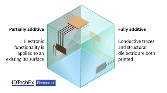
Research firm IDTechEx divides the technology landscape for 3D electronics into two broad categories: partially additive and fully additive. Image courtesy of IDTechEx.
The Challenge of 3D Electronics
AM is a three-pillar concept of materials, processes and design.
“The long-term goal is to load up a design file and see the board, the chips and the peripheral product,” says Zachariah Peterson, owner of Northwest Engineering Solutions. There are challenges: “Today printed electronics are all planar. Until we can print semiconductors as 3D elements, we can’t reach the level of fully printing 3D electronic products.”
3D printing won’t replace complementary metal oxide semiconductor manufacturing “for a long time,” Peterson notes. But semiconducting polymers are becoming available. Radio frequency electronics are closer, where arbitrary shaped non-planar objects can be fully 3D printed. “We can do much with RF printed circuits that can be printed to an arbitrary shape.”
Recently in a research lab (undisclosed for competitive reasons), 3D printing was used to create a semi sphere from laminates with an antenna. This is an example not of a mechanical electronics product, but it is the 3D printing of a device with electronics.
As Peterson notes, “It must at some point connect to another device. It is a peripheral that connects back to a circuit board. That’s the state of the art of assembly.”
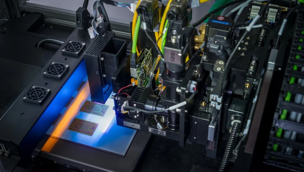
Peterson says the current leader in commercializing 3D printing is Nano Dimension, a well-funded startup based in Florida.
“Nano Dimension is the world’s only multi-material, layer-by-layer electronics 3D printing,” says Sean Patterson, CIO. “Everyone else who does printed electronics puts metal on the outside of things, like painting. They don’t have dual materials, so they can’t do complex circuitry.”
Additively Manufactured Electronics
Nano Dimension was founded as a research lab spin-off in Israel in 2012; it now has research offices in Boston and Florida. The company manufactures DragonFly Pro, a multimaterial, multi-layer 3D printer that Patterson says can generate entire circuits in one step, “including substrate, conductive traces and passive components.”
An early DragonFly customer was Piezoskin S.R.L., an Italy-based micro-electromechanical systems (MEMS) specialist. The company used DragonFly to develop a 3D-printed sealed packaging with electrical pads. The printed electronics package has the electrical pads directly printed onto metal layers on which an RF connector is soldered.
“The ability to transfer electric pads in a sealed package is one of the most crucial parts in ohmic-contact microelectromechanical systems, as it determines the device performance and reliability, particularly for soft and flexible devices where the electrical connectors are typically difficult to produce,” according to Nano Dimension.
“Nano Dimension’s AME technology helped us to achieve an original product prototype in which wires and connectors were eliminated such that the package was minimized to obtain an optimal user experience. It simplifies the manufacturing process compared to traditional manufacturing methods,” says Francesco Guido, CTO of PiezoSkin.
Having perfected a methodology, Guido says PiezoSkin can now customize printed packages with flexible transducers.
The Problem with Software
Even if most people don’t know how a 3D printer works, they understand three-dimensional objects.
“A sculptor understands 3D, so does a kid using LEGO bricks,” says Patterson. “Electronics are different—it is not intuitive. Only electronics engineers really get it.” And electronics engineers use 2D CAD, “which limits the design of products.”
To complicate things further, Patterson says, “there are more standards [to follow] in electronics than in all of mechanical design. To create 3D printing in electronics is a revolution, not an evolution. From an initial design to the OEM [original equipment manufacturer], it is a completely different challenge.”
Now there is a gulf between electronics CAD (ECAD) products for electronics design and mechanical CAD (MCAD) products. There is no one CAD solution that can design a full 3D electromechanical part to be sent to a 3D printer. Nano Dimension has created pre-processing software called Switch, which enables engineers to prepare PCB designs for 3D printing on the DragonFly.
Switch accepts the two most common file formats in ECAD, Gerber and Excellon. It then creates multilayer 3D files from either. The software adjusts parameters including layer order and thickness, then prepares the file to be loaded directly into DragonFly.
There are limitations and new workflows to be developed. ECAD products have large libraries of common electronics components, but these aren’t compatible with MCAD. Nano Dimension offers a utility to import ECAD work into Dassault Systèmes SolidWorks, which allows a mechanical designer to work with the shape and explore options.
The goal is to create finished electromechanical products straight off the 3D printer. Nano Dimension works with Mass Robotics, a nonprofit innovation hub in Boston for robotics and artificial intelligence. “People try to fit a flat circuit board to an object [in robotics]. What if you could print the electronics for the robot elbow when you print the elbow?”
For the leading MCAD vendors, 3D electronics is somewhere on the roadmap, but there is nothing ready to ship. Autodesk Fusion R&D is working on adding electronics design to the platform, but additive manufacturing that includes 3D printed electronics isn’t yet on the agenda.
“Fusion is excellent for design and print, like bases for circuit boards,” notes Edwin Robledo, the technology marketing manager for Fusion 360 electronics at Autodesk. But at what point will Fusion combine the part and its electronics in one design environment? “It will come. We can now lay out a circuit board and create a model,” Robledo notes. Previously designed circuit boards can be imported and used as a part in the model, but there is not yet a facility for integrating the physical and the electronic.
Jay Tedeschi at PTC says his company prefers to partner with domain experts than to acquire new technology to make 3D electronics design a reality. He describes a new Onshape add-on, PCB Studio, as an example of what the company will provide. “PCB Studio is essentially a handshake product,” connecting MCAD and ECAD design. “It allows MCAD guys to define an envelope, then send the information to the ECAD guys.”
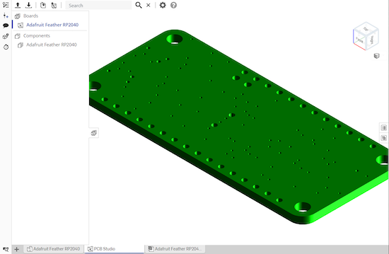
Onshape PCB Studio, a free add-on, imports ECAD file data into an Onshape project. It allows the user to create parts and assemblies, using the PCB data as a reference. Image courtesy of PTC.
Looking ahead, Tedeschi says the next hurdle for CAD software is to match the worlds of flexible circuits and flat boards. The IDX standard for PCB layout exchange between MCAD and ECAD now supports flexible boards, such as those needed in foldable cell phones or laptop hinges. “The next revolution in 3D printing will be hard and flexible integrated electronics. Software won’t be the limiting factor, it will be 3D printing itself. I have to believe that in two years we will see this stuff take off.”
Randall S. Newton is principal analyst at Consilia Vektor, covering engineering technology. He has been part of the computer graphics industry in a variety of roles since 1985. Contact him at DE-Editors@digitaleng.news.
More Onshape Coverage
More PTC Coverage
Subscribe to our FREE magazine, FREE email newsletters or both!
Latest News
About the Author
Randall S. Newton is principal analyst at Consilia Vektor, covering engineering technology. He has been part of the computer graphics industry in a variety of roles since 1985.
Follow DE