Microfabrica: Mass Production at Millimeter Scale

This articulating tissue scaffold was produced with Microfabrica’s proprietary production method. Image courtesy of Microfabrica.


Latest News
December 1, 2016
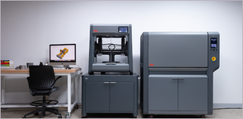
The 40,000-sq.-ft. manufacturing space in Van Nuys, CA, looks like any other small fab, or computer chip fabrication plant. Although the equipment used for photolithography, electrodeposition and the rest are the same, the products created by Microfabrica are very different.
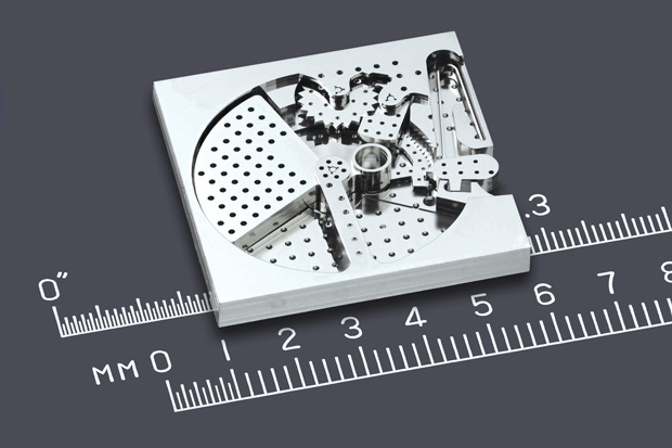 A munition timing device that was printed as a single part and significantly scaled down. Image courtesy of Microfabrica.
There’s no silicon, for starters. Instead, the 4-6 in. wafers on which Microfabrica’s products are built are made of ceramics and designed for reuse. Instead of chopping up these wafers as in the creation of computer chips, technicians essentially wash them off at the end of the manufacturing process and start again. And what comes out in the wash are like nothing else. They are vanishingly small—in many cases less than a millimeter in diameter—and only a few millimeters across. They separate from each wafer by the hundreds, the thousands and even ten thousand at a time. They take the form of tiny medical forceps, mechanical timing mechanisms complete with moving clockwork, novel computer chip cooling devices and more.
“We are the only high-volume production, additive manufacturing platform in the market,” says CEO Eric Miller. “We’re focused on another end of the spectrum from where a lot of the 3D printing companies are focused, and that’s at the micro scale.”
Not only are the devices and components made by Microfabrica smaller than those made by other processes, but they are also made of high-grade metals, rendering them suitable for use in production applications as well as the prototyping that is common to 3D printing. Carol Livermore, professor of mechanical and industrial engineering at Northeastern University, is among the experts impressed by Microfabrica. “If the user needs the material properties of a metal, then Microfabrica’s technique would provide what silicon micromachining can’t,” she says. “This can fill an important need for rapid development and robust manufacture.”
3D Printing, Semiconductor Style
Company president and chief operating officer Michael Lockard started Microfabrica with fellow 3D Systems alumnus Adam Cohen in 2000 with seed money from a DARPA grant. The two initially planned to develop micro 3D printers. “We ultimately realized that’s not the right platform for this technology,” Lockard says now. “The best embodiment for this technology is to leverage the full panoply of semiconductor tools to embody it as a fab.” (Cohen has since gone on to direct the Laboratory for Additive Manufacturing, Robotics and Automation at Southern Methodist University.)
The Van Nuys headquarters for the 100-employee company includes the manufacturing facility and offices for some of the company’s 30 or so engineers and scientists. They collaborate with customers to design parts as well as complete devices. Customers include major medical device manufacturers and aerospace firms.
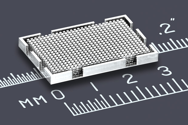 This thermal management device showcases the fine details possible with Microfabrica’s process. Image courtesy of Microfabrica.
The design and manufacturing process typically starts with a CAD file sent by a customer to Microfabrica engineers, who will then help refine the design. From there, the reworked design gets put through Microfabrica’s own proprietary software that slices the design into anywhere from four to over 50 slices that can range from 5-50 microns thick.
Finally, the designs are output to the fab for a series of processes any semiconductor device manufacturer would recognize: photolithography, in which patterns are created on the wafers; electrodeposition, in which layers of material are applied according to the patterns; and planarization to smooth each layer. More than one design can be made on each wafer at once.
Small Devices, Large Production
Livermore says she knows of no 3D printing process that can exceed the level of detail produced by Microfabrica. A typical polyjet printer may produce individual layers of plastic as small as about 16 microns thick. Direct metal sintering—the process that is perhaps most like Microfabrica’s in that it produces metal parts—forms layers that may be 20 or so microns thick.
The benefits are just being realized by Microfabrica’s customers, says Miller, because they often don’t know what the process, dubbed MICA freeform, can really do until they start working with it. Miller cites as an example a manufacturer that went to Microfabrica to produce a very small gear for a miniature pump. After some back and forth, Microfabrica ended up fabricating the entire gear assembly with all of its moving parts in a single step, instead of just the one gear that the customer itself would have needed to put together with the parts of the previous design.
Besides helping its customers create products, Microfabrica is developing its own devices at an R&D center in Santa Clara, CA. These include tissue dissection and tissue removal devices. The company plans to market them to manufacturers to sell under their own brand names.
 This articulating tissue scaffold was produced with Microfabrica’s proprietary production method. Image courtesy of Microfabrica.
Once products have been manufactured at Microfabrica’s Van Nuys facility, it’s time to ship them off to customers. Packaging varies according to the products being made and each customer’s needs, says Lockard. After being filtered from the chemical bath that separates them from the wafer, the devices might be packed in gel or placed in vials of alcohol for shipping. Because each device can cost anywhere from $1 to $100, a single small vial or gel pack can contain tens of thousands of dollars’ worth of products. For this company at least, size does matter.
More Info
Subscribe to our FREE magazine, FREE email newsletters or both!
Latest News
About the Author
Michael Belfiore’s book The Department of Mad Scientists is the first to go behind the scenes at DARPA, the government agency that gave us the Internet. He writes about disruptive innovation for a variety of publications. Reach him via michaelbelfiore.com.
Follow DE